Hexagonal Boron Nitride (h-BN) on Si/SiO2
hBN on Si/SiO2
Product Detail
1. Preparation Method
CVD Method
2. Characterizations
|
|
Monolayer h-BN/hBN |
|
Transparency |
> 97% |
|
hBN Coverage |
100% with sporadic adlayers |
|
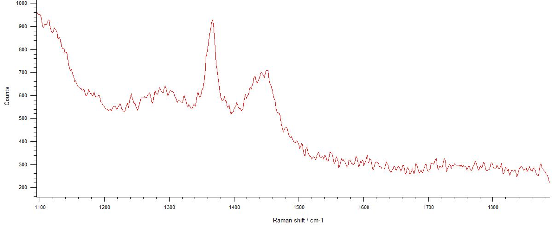
Raman Peak |
1370 /cm-1 |
|
Bandgap |
5.97 eV |
|
Grain size |
>4 μm |
|
h-BN thickness |
monolayer (0.333nm theoretical) |
|
|
Si/SiO2 Substrate |
|
Type/Doping |
P/B |
|
Wafer Thickness |
500 +/- 50 μm |
|
Oxide Thickness |
300 nm |
|
Resistivity |
1-10 (Ω -cm) |
|
Orientation |
<1-0-0> |
|
Growth Method |
CZ |
|
Metal Impurities |
1.00e10 – 5.00e10 (at/cm2) |

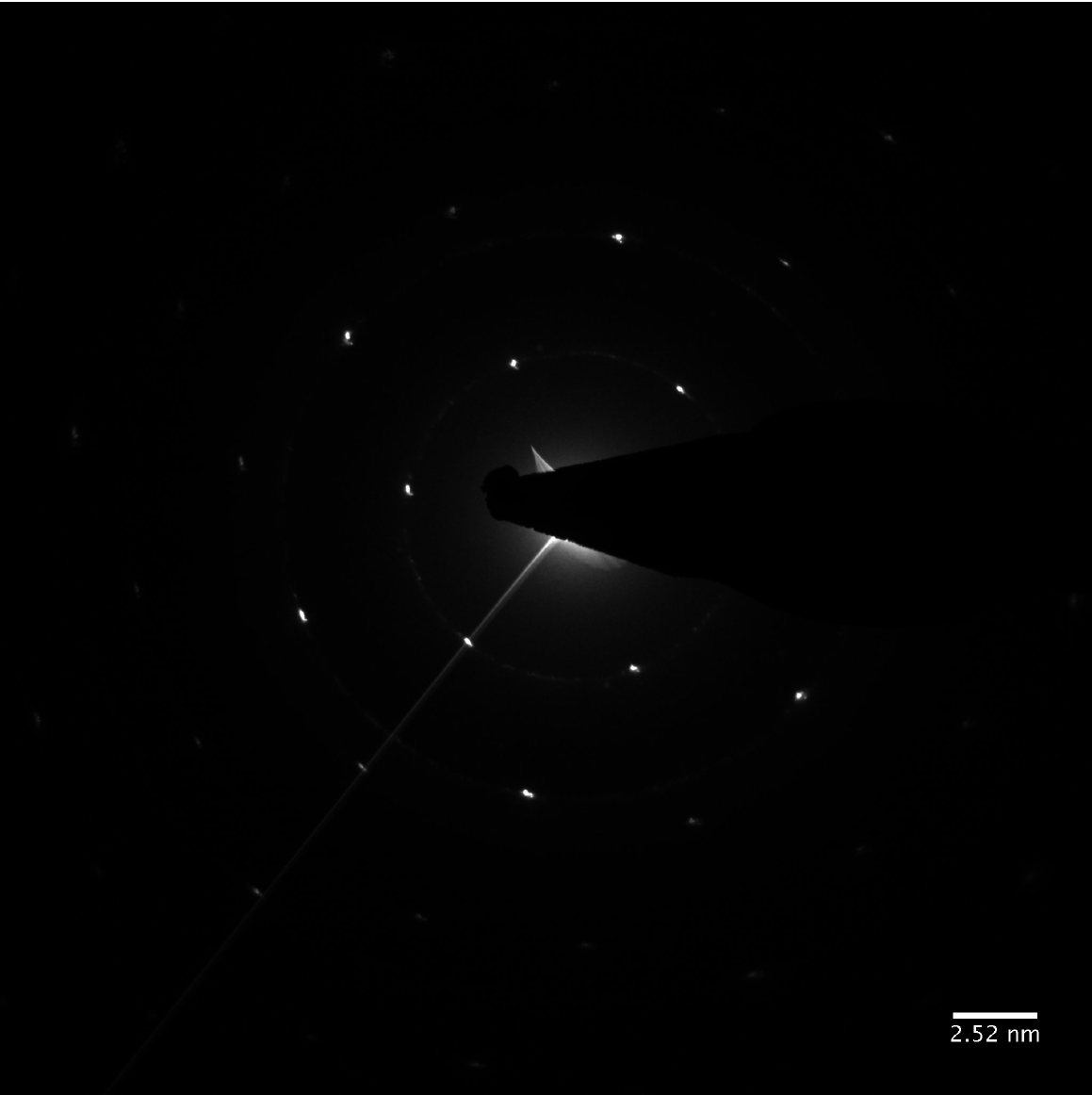
Typical Crystal Diffraction Image of ACS Material Monolayer h-BN

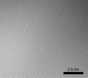
Typical TEM Image of ACS Material Monolayer h-BN

Typical Raman Spectrum of ACS Material Monolayer hBN
* The indicated product metrics are generic to our transfer process. For all ACS Material products, the displayed range represents electronic data that we have obtained using our in-house transfer capabilities to transfer hBN to SiO2. Your own metrics will depend entirely on the transfer methods that you use, and the resultant quality of your transfers.
3. Application Fields
1) Proton conductors
2) Fuel cells
3) Water electrolysis
4) Graphene-based devices
4. User Instruction
To ensure the maximum shelf life of your graphene sample, it is best stored under vacuum or in inert atmosphere (Argon or Nitrogen) conditions once the vacuum sealed package has been opened.
Disclaimer: ACS Material LLC believes that the information on our website is accurate and represents the best and most current information available to us. ACS Material makes no representations or warranties either express or implied, regarding the suitability of the material for any purpose or the accuracy of the information listed here. Accordingly, ACS Material will not be responsible for damages resulting from use of or reliance upon this information.
FAQ
1. Do the sizes refer to the wafer or h-BN coverage or both?
Both. The wafers for this material come in 4, 6 or 8 inch diameter rounds and the h-BN covers 100% of each wafer on one side.
